Introduction
The cencept of a phototransistor has been recognized for numerous years. It was proposed by William Shockley in 1951 after the discovery of the normal bipolar transistor. Just two years later, a phototransistor was demonstrated, marking a major step in its development.
This device can detect light levels and changes in current flow between the emitter and collector terminals. Its applications span across electronic circuits, often available at low cost from distributors of electronic components, making it widely obtainable and continued in use for different practical needs.
What is a phototransistor?
A phototransistor is a semiconductor device that reacts to light by allowing current to flow. Unlike regular transistors, it has an exposed base that receives light instead of an electrical signal. This design enables it to detect particles of energy, making it ideal for various applications. Its ability to respond to infrared and visible radiation makes it highly effective in electronic circuits.
The structure of a phototransistor is optimized for photo operations, improving its performance. It typically includes a larger collector and base width, created using diffusion or ion implantation. This design enhances gain and proportional response to pulses of light, improving efficiency. Such features are valuable in digital signals and electrical systems that require accurate detection.
In practical use, phototransistors are capable of functioning like photoresistors (also called LDRs) but offer better control. They can both convert and amplify light signals into voltage or current, unlike photoresistors that only adjust resistance. This makes them an essential component in systems that require precise switching and activation based on radiation levels.
Commonly found in Darlington’s, diodes, and TRIACs, phototransistors are widely used in devices that rely on low-cost electronic solutions. Their ability to handle reverse flows of current enhances their reliability. Whether used for converting light signals or improving dependence on electric inputs, these versatile devices play a vital role in modern technology. You can also read difference between BJT and FET.
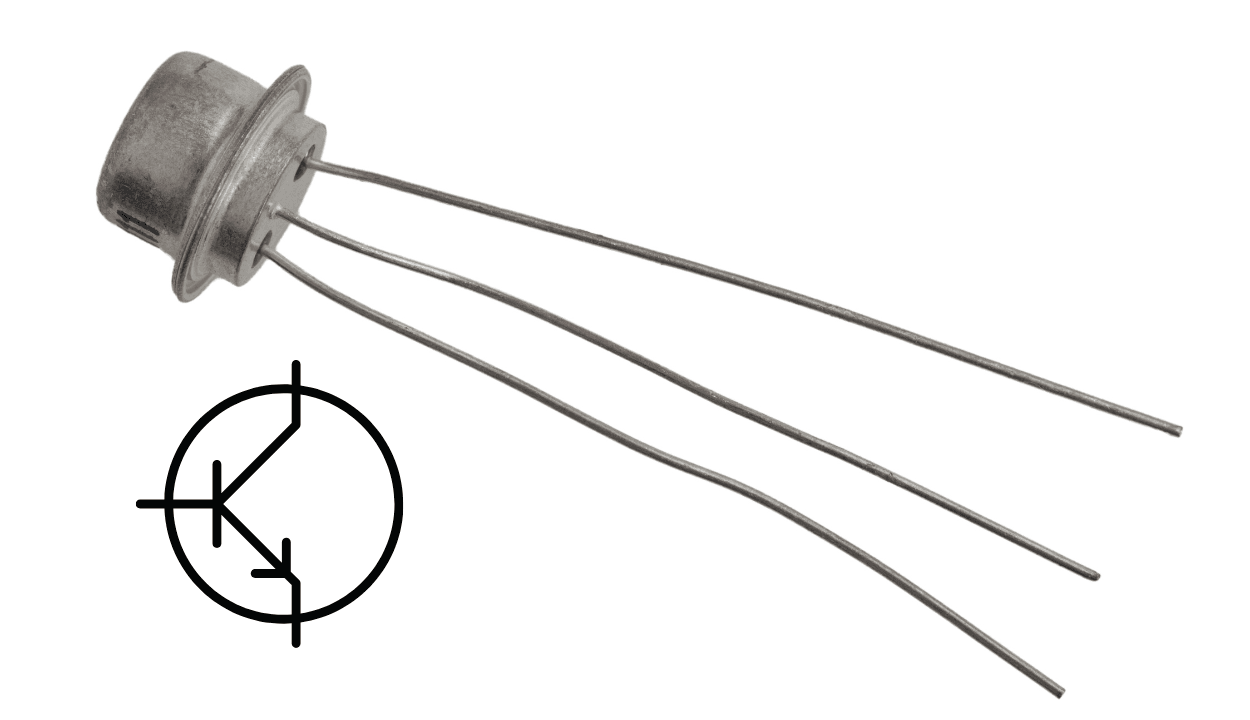
Phototransistor diagram
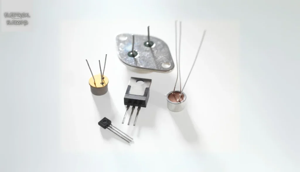
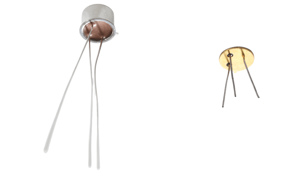
Construction of Phototransistor
A phototransistor is a special device designed to react to illumination. It includes a collector-base junction that is extremely sensitive to incident photons. This allows the current flow to increase significantly when light strikes the surface. Its gain can reach hundreds or even several thousand, making it highly efficient.
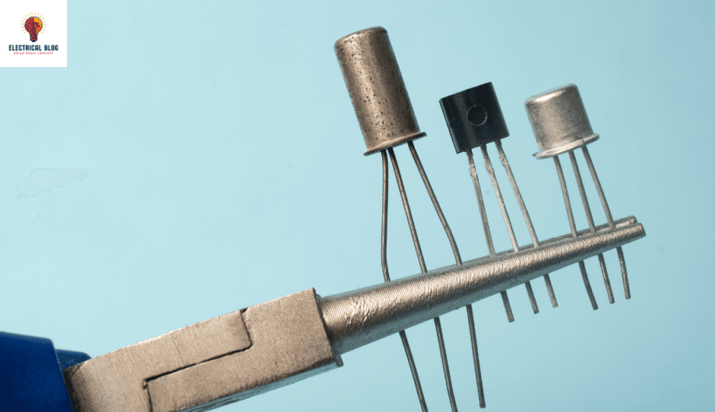
The construction of a phototransistor often includes bipolar materials like silicon, gallium, or germanium for improved high-efficiency performance. Modern components use advanced materials for better voltage control and reduced noise levels. Designs may feature P-N-P or N-P-N configurations depending on the application. The resistor and load help manage the voltage drop effectively.
In practical design, the base-emitter region may be left open to enhance sensitivity. This open design improves amplified results by allowing thermally generated pairs to boost the current gains. The controller mechanism ensures precise action, regulating positive or negative voltage responses.
Ancient designs relied on conventional materials, but modern advancements have improved levels of performance. By activating the gate, the phototransistor efficiently handles electrical outputs through the outlet. With proper connection, these devices provide stable supply conditions, ensuring improved results in working environments.
How does a phototransistor work?
A phototransistor works by reacting to light that strikes its base. This activates the flow of current between the emitter and collector terminals. As the current increases, it becomes concentrated and is then converted into voltage for the circuit.
Unlike normal transistors, a phototransistor is generally designed with a disconnected base connection. Instead of an electrical signal, hole-electron pairs are formed by light, allowing flow through the BE junction and collector terminal. The supply is managed through a reverse-biased configuration, ensuring stable performance.
Phototransistor symbol
Types of phototransistors
A BJT phototransistor is designed to work in low-light conditions. In the absence of light, it may allow leakage of around 100 nA between the collector and emitter. However, when exposed to a beam, it can perform up to 50 mA, distinguishing it from a photodiode.
The FET phototransistor operates with terminals that connect internally via the source, drain, and collector. The base reacts to light and controls the current flow, allowing for better performance in varying conditions. This type of transistor effectively manages current when activated.
Phototransistor Circuit
A phototransistor is a device that works like a normal transistor but responds to light. Instead of relying only on a base signal, its current is multiplied based on the visible or infrared light it detects. With just two pins, it efficiently controls the collector current in a circuit for reliable performance.
In a simple diagram, the Vout terminal is connected to the resistor, where the voltage can move high or low depending on the light levels. The controlled output responds to the incident wavelength across a broad range, like near UV, near IR, or the visible spectrum. This allows the phototransistor to adapt to different lighting conditions.
For enhanced performance, an op-amp may be added to boost the signal, ensuring better accuracy in complex systems. This setup is common in microcontroller circuits that require precise input detection. Additional designs may include optical switches, optoisolators, or retro sensor configurations for improved gain and output control.
Amplification of Phototransistors
The phototransistor is highly sensitive and performs well in low-light conditions. Its operation mainly depends on the applied light intensity, where the input at the base terminal controls the current. As incident photons hit the surface, the transistor’s gain helps produce a strong current gain.
For improved amplification, a photodarlington-type design can be used to enhance performance. This setup provides extra gain, delivering stronger output by combining two transistors. With this method, the net gains can reach higher values, exceeding 100,000 A, making it far more sensitive than a photodiode.
Although the phototransistor offers better response and a wider range, it may still generate noise at certain levels. The connected emitter and terminal manage this effectively, ensuring stable performance in normal circuits. This structure improves both signal clarity and amplified output for demanding applications.
Modes of Operation
A phototransistor works in two modes: active and switch mode. The switch type is commonly used in circuits, working in an ON/OFF system where no light means no current flow. As exposure to light increases, the supply of current starts. The active mode, also called linear, reacts in a proportional way to the light stimulus, ensuring a linear response when needed.
Performance Specifications of Phototransistors
It must be chosen carefully based on key parameters for optimal performance.
Collector Current (IC) defines the maximum current that the transistor can handle without damage.
Base Current (Iλ) controls the transistor’s activation when light is applied.
The Peak Wavelength shows the optimal light frequency for the best response.
Collector-to-Emitter Breakdown Voltage (VCE) ensures that the transistor can withstand high voltages.
Collect-Emitter Breakdown Voltage (VBRCEO) indicates voltage limits for safe operation.
Emitter-Collector Breakdown Voltage (VBRECO) defines the reverse voltage limit for the emitter side.
Dark Current (ID) is the small leakage current that occurs even without light exposure.
Power Dissipation (PD or Ptot) reflects the maximum energy that the phototransistor can handle.
Rise Time (tR) and Fall Time (tF) determine the response speed to light changes.
Design Parameters of Phototransistors
The phototransistor design depends on selected materials and composition for better sensitivity. Homo-structure devices use a single material like silicon and achieve gain levels between 50 and several hundred. On the other hand, heterostructure devices use several materials for higher gain, up to 10k, but are less common due to high production costs.
For proper functioning, mounting technology like SMT or THT is crucial. SMT involves placing components on a PCB by connecting terminals through soldering. The PCB pad may be coated with paste, which melts under high temperatures using an infrared oven to secure the pads. THT allows components to be placed through holes on the PCB and soldered on the opposite side.
Electromagnetic Wavelength Range
Silicon (Si): 190 to 1,100 nm
Germanium (Ge): 400 to 1,700 nm
Indium Gallium Arsenide (InGaAs): 800 to 2600 nm
Lead Sulfide: Less than 1000 to 3500 nm
Characteristics of Phototransistors
Low-cost design makes phototransistors suitable for budget-friendly applications.
Supports visible and near-IR photodetection for diverse light-detection needs.
Provides gains ranging from 100 to over 1,500, enhancing performance.
Ensures moderately fast response times for effective signal detection.
Available in a wide range of packages, such as epoxy-coated, transfer-molded, and surface-mount technology options.
Advantages and Disadvantages of Phototransistors
Advantages
They generate a higher current than photodiodes, improving performance.
They are inexpensive, simple, and small, allowing for easy integration into an integrated computer chip.
Known for their fast response time, they provide nearly instantaneous output in light detection.
Unlike photoresistors, phototransistors can produce voltage as well as current.
Disadvantages
They made of silicon are not capable of handling voltages above 1,000 volts.
They are more vulnerable to surges, spikes, and sudden electrical fluctuations.
Exposure to electromagnetic energy can affect its performance and reliability.
Phototransistors restrict electrons from moving as freely as devices like electron tubes do.
Applications of Phototransistors
Security systems use phototransistors to detect movement and trigger alarms.
In computer logic circuitry, they help manage signal processing and control operations.
IR detectors rely on phototransistors for sensing photo signals in remote controls and sensors.
Punch card readers utilize phototransistors to read data patterns in card systems.
Encoders use them to measure speed and direction in motors and control systems.
Electric controls employ phototransistors to regulate devices and automate tasks.
Relays incorporate phototransistors to control power flow in circuits efficiently.
Lighting control systems, such as those used on highways, rely on them for automated light adjustments.
In level indication systems, they monitor fluid or material levels in tanks and containers.
Counting systems use phototransistors to count objects moving along conveyor belts or production lines.
Photodiode Vs Phototransistor
| Feature | Photodiode | Phototransistor |
|---|---|---|
| Function | A Photodiode is a PN-junction diode that generates electric current when light or a photon hits its surface. | A Phototransistor is designed to change energy from light into electrical energy. |
| Sensitivity | Less sensitive to light detection. | More sensitive to light exposure. |
| Output Response | Provides a fast output response for quick signals. | Offers a low output response, making it slower. |
| Output Type | Produces only current as its output. | Produces both voltage and current outputs. |
| Applications | Used in solar power generation, UV/IR detection, and light measuring devices. | Commonly used in compact disc players, smoke detectors, and lasers. |
| Reactivity | More reactive to incident lights for faster response. | Less reactive to light, making it slower to respond. |
| Dark Current | Produces less dark current, reducing noise levels. | Generates high dark current, which may increase noise. |
| Biasing Type | Uses both forward biasing and reverse biasing for flexibility. | Operates only on forward biasing. |
| Linear Response Range | Offers a wider linear response range for stable performance. | Has a lower linear response range, making it less stable. |
| Current Handling | Allows low current output, limiting power capacity. | Supports high current flow for stronger signals. |
| Power Efficiency | Ideal for battery-powered devices that consume less power. | Functions as a solid-state switch, enhancing power handling for specific needs. |
Conclusion
They are versatile electronic components widely used for their ability to convert light into electrical energy. They offer advantages like higher current, fast response, and suitability for low-cost applications. Phototransistors are crucial in modern technology. They are used in various applications, including security systems, IR detectors, computer logic circuits, and lighting control.
Despite their benefits, they have limitations such as high dark current and vulnerability to voltage surges, which should be considered during design. Engineers can improve systems by knowing the features, performance specs, and uses of phototransistors.