Introduction
I first studied the transistor during my electronics course, where the concept of current flow and signal amplifier design caught my attention. The three-terminal device made of p-type and n-type layers forms a p-n junction, helping to amplify weak signals. A small current at the base can control a large flow between the collector and emitter, which I found fascinating.
Introduced in 1951 at Bell Laboratories by Dr. Shockley, the Bipolar Junction Transistor remains key in modern semiconductor systems. I’ve worked with both types, Field-Effect Transistor and BJT, but the built-in transistors, bias resistors, and semiconductor device structure in the Bipolar Junction Transistor stand out for their use. The objective of magnifying signals using transistors made from silicon across different regions, junctions, and terminals is a core skill that every engineer should learn.
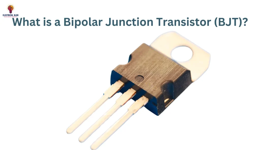
What is a bipolar junction transistor (BJT)?
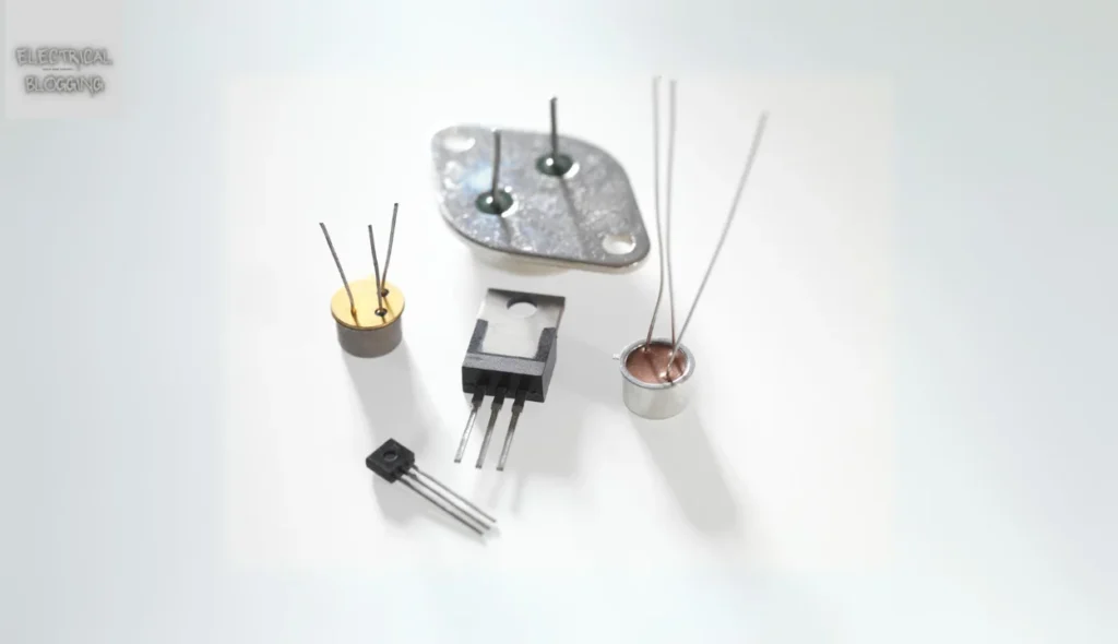
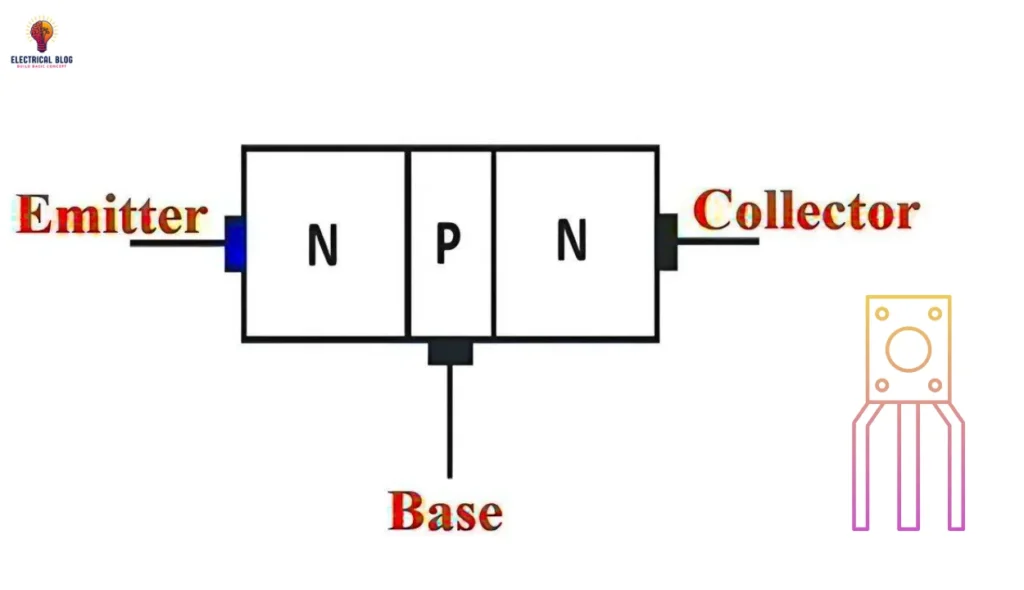
A bipolar junction transistor is a three-terminal semiconductor device made of two p-n junctions, used to magnify a small signal. The base, collector, and emitter are its terminals, and a small amplitude input at the base gets amplified at the collector. It is a current-controlled device, and an external source like a DC power supply is required for the amplification process. I remember experimenting with a bipolar junction transistor in a lab where I saw firsthand how the signal amplification worked through the transistor.
Read more: 2N2222A transistor
Bipolar Junction Transistor symbol

Construction of BJT
In my early electronics training, I learned how a bipolar junction transistor is formed using semiconductors and p-n junctions. It has three key parts: emitter, base, and collector, carefully placed and designed for better current control. The junctions help divide the transistor into these parts, each having a unique role.
Emitter
The emitter is the outermost layer, usually heavily doped with semiconductor material to push carriers into the base. Depending on the type, N-type or P-type material is used. In an NPN transistor, the emitter uses N-type, while in a PNP transistor, it uses P-type.
Base
The base is the intermediate layer, made from different materials than the emitter, and is slightly doped. It forms a narrow zone between the emitter and collector and acts as a control gate. Whether it’s a PNP transistor or an NPN transistor, the base works as the central path for signals.
Collector
The collector is the inner layer with a modest doping level, often made from the same material as the emitter. In an NPN transistor, it is N-type, and in a PNP transistor, it is P-type. This part gathers the current and completes the transistor’s function.
Two junctions are very important: the emitter-base junction, which is forward-biased in normal operation, and the collector-base junction, which is reverse-biased. These junctions manage how current moves across the transistor, ensuring stability and control in electronic design and circuit creation.
Operation of BJT
Active region
In the active region, the transistor functions as an amplifier. The emitter-base junction is in a forward-biased state, whereas the collector-base junction is in a reverse-biased state. Here, the collector current (IC) is proportional to the base current (IB) and is controlled by it, expressed:
IC = βIB
Saturation region
When the BJT operates in the saturation region, both the emitter-base junction and the collector-base junction are forward-biased. In this on state, the transistor conducts fully, and the collector current becomes dependent on VCE, which is just a few tenths of a volt. This mode is useful for transistor switches in digital circuits.
Cut-off region
In the cut-off region, the emitter and collector junctions are in reverse bias, so the transistor is off. Almost no current flows from collector to emitter, and IC becomes zero (IB = 0, IC = 0). I’ve tested this behavior in labs and seen how current stops completely when the BJT is in the cut-off region.
Types of BJTs
NPN Transistor
PNP Transistor
NPN Transistor
In an NPN transistor, P-type material is placed between two n-type semiconductors, which act as the emitter and collector. The base is p-type, and during the forward active state, the emitter-base junction is forward biased, while the collector-base junction is in reverse bias. When voltage crosses the barrier potential (about 0.3 volts for germanium transistors and 0.7 volts for silicon transistors), current starts to flow.
From the N-type emitter, free electrons move toward the base region, generating emitter current. A few electrons combine with holes in the base, creating base current, but most move to the collector region, producing collector current. A small part of this includes reverse saturation current from thermally generated carriers, and the width of the base ensures minimal recombination with holes, keeping conventional current efficient.
Read more: Difference Between BJT and FET
PNP Transistor
In a PNP transistor, two P-type semiconductors are placed on each side of an n-type material, forming the PNP BJT. The base is n-type, whereas the emitter and collector are P-type. Current flows due to the movement of holes, unlike free electrons in an NPN transistor.
The emitter-base junction is in a forward bias state, whereas the collector-base junction is in a reverse bias state. Holes from the emitter area flow into the base region, forming emitter current. Some holes combine with electrons, creating base current, but most reach the collector region, producing collector current and a small reverse saturation current from thermally generated carriers due to recombination and narrow base width.
The bipolar junction transistor is a current-controlled device, but the voltage between its terminals plays a key role in its behavior.
Voltage control
Through voltage control, especially at the base-emitter junction voltage, we can turn the transistor on or off. This voltage directly affects the input and how current flows from the emitter to the collector.
Charge control
In charge control, electrons or holes act as charge carriers within the base region or base area, depending on NPN transistors or PNP transistors. A smaller current at the base (IB) controls a much larger collector current (IC). This makes the BJT very effective as a switch or amplifier.
Current Flow
The current gain of the device, shown as β, tells us how much IC increases with IB. The total output current includes emitter current (IE) and follows the equation IC = β * IB. From my own work in labs, understanding current flow, collector, and emitter behavior helps optimize any BJT-based circuit design.
Bipolar Transistor Configurations
Common Base Configuration
Common Emitter Configuration
Common Collector Configuration
Common Base Configuration
In common base characteristics, the base of the transistor is grounded, with input at the emitter and output from the collector. The emitter-base junction is biased forward, while the collector-base junction is reverse biased. The CB arrangement offers low voltage gain but high current gain, making it useful in impedance matching. It also inverts the phase of the output signal relative to the input, acting as a buffer in circuits with high impedance and low impedance. I’ve used this in high-frequency applications like RF amplifiers, where stable signal performance is essential.
Common Emitter Configuration
In common-emitter characteristics, the emitter is grounded, the base works as input, and the collector provides the output. The CE configuration, like the CB configuration, has a forward-biased BE junction and a reverse-biased CB junction. The relation between voltages is shown as VCE = VCB + VBE or VCB = VCE – VBE.
The emitter current (IE) is the sum of IC and IB, which means IE = IC + IB. The CE configuration offers a good voltage gain and a modest current gain, often useful in voltage amplification. It also causes a phase relationship shift, flipping the phase of the input signal relative to the output.
Common Collector Configuration
In common collector characteristics, the collector of the transistor is grounded, with the base as input and the emitter as output. The CC setup gives low voltage gain but high current gain, working best as a buffer for current. It helps maintain the identical phase between signals, preserving a stable phase relationship.
This configuration supports impedance transformation, impedance buffering, and voltage following to match impedance between circuits. I’ve personally used it for clean signal transitions in sensitive audio setups, where impedance handling is critical.
Functions of BJTs
Junction Bipolar Transistors (BJTs) play a vital role in amplification by increasing electrical signals. They magnify weak input current at the base to control higher current flow between the collector and emitter. I often use BJTs in audio amplifiers to strengthen sound signals in my projects.
BJTs are also used for switching, working like electronic switches to regulate current flow. In digital circuits and logic gates, a small base current acts like a trigger to switch the current path. This makes them perfect for fast-response systems.
In signal modulation, BJTs help alter carrier signals in modulation circuits. These are key in information transmission within communication systems, changing signal amplitude, frequency, or phase. I’ve personally seen how adjusting the base signal can shape entire communication outputs.
Advantages of BJTs
Voltage gain is high, making BJTs great for amplification tasks.
They ensure good performance even in high-frequency operations.
BJTs support a wide gain bandwidth, enhancing signal response.
They operate well in high-frequency operations without signal loss.
The forward voltage drop is low, which improves energy efficiency.
Maximum current density allows them to handle more current in small areas.
Suitable for both low-power and high-power applications, it offers design flexibility.
Disadvantages of BJTs
Less switching frequency makes it difficult to use BJTs in high-speed switching circuits.
Noise production is greater, which can affect signal clarity in sensitive designs.
Thermal stability is lower, causing performance issues at varying temperatures.
The time taken for switching is not fast, especially compared to the high flashing frequency of voltage and current in modern systems.
Applications of BJTs
BJT is widely used as an amplifier to boost weak signals in audio and communication systems.
It also works effectively as a switch in automation, digital electronics, and control systems.
BJT functions as an oscillator, producing continuous waveforms in RF and signal generation circuits.
It is applied in logic circuits, helping with decision-making tasks in digital systems.
Clipping circuits use BJTs to limit or modify the waveform of input signals.
BJT also acts as a demodulator and detector in radio and data communication systems.
It is commonly found in temperature sensors, ensuring thermal-based circuit adjustments.
Conclusion
Bipolar Junction Transistor is a key component in electronics, serving as an essential element in most electronic circuits. With its three-layer structure—emitter, base, and collector—it can operate circuits, amplify, and switch with ease. Its simplicity, reliability, and detailed concepts make it the foundation of many complex circuits.
Whether used as an amplifier to enhance signals or as a switch, the Bipolar Junction Transistor handles power efficiently across three regions. It offers flexible configurations and performs the amplification process without needing any external sources. In my experience, it is an important component that continues to shape modern circuit design.