
BGA rework is one of those PCB assembly topics that sounds simple until a real board is sitting on the bench. In theory, the process is straightforward: remove the defective BGA, clean the pads, replace or reball the package, reflow it again, and verify the joints. In practice, the success of BGA rework depends on board design, package type, thermal history, pad condition, component availability, and the skill of the technician doing the job.
For prototypes and low-volume builds, BGA rework can save a board, recover an expensive assembly, or keep an engineering schedule moving. For production hardware, however, repeated BGA rework can become a warning sign. It may point to deeper issues in stencil design, thermal profiling, PCB warpage, moisture control, or component handling.
This article explains what BGA rework really involves, where it usually fails, and how to decide whether a board should be reworked or rebuilt.
What BGA Rework Actually Means
A Ball Grid Array, or BGA, is a package where solder balls are located underneath the component instead of visible leads along the sides. This structure allows higher I/O density and better electrical performance than many traditional leaded packages, but it also makes inspection and repair more difficult.
With a QFP or SOIC package, a technician can usually see the solder joints directly. With a BGA, the solder joints are hidden under the package body. That means visual inspection is limited, and X-ray inspection is often required to confirm whether the joints are acceptable.
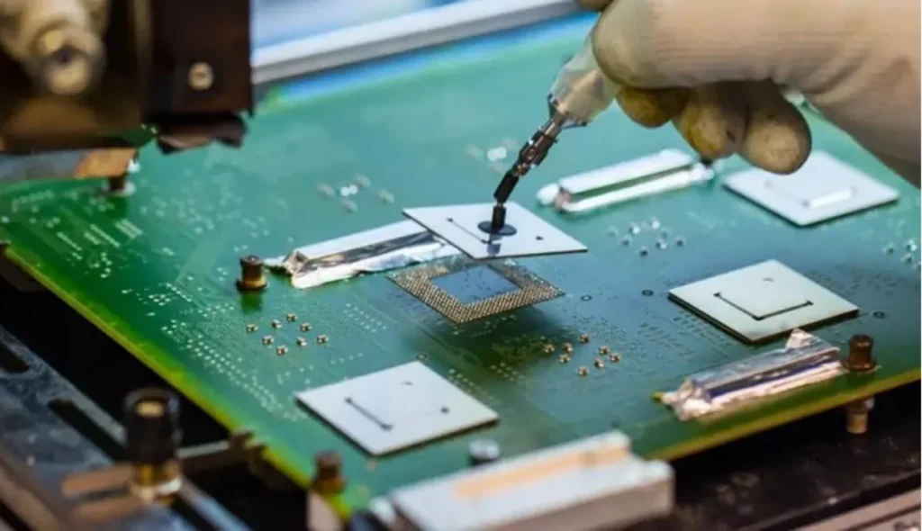
A typical BGA rework process includes:
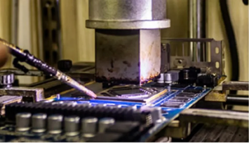
- Localized heating of the BGA package and PCB area
- Removal of the component after solder reflow
- Cleaning residual solder from PCB pads
- Inspection of pad integrity and solder mask condition
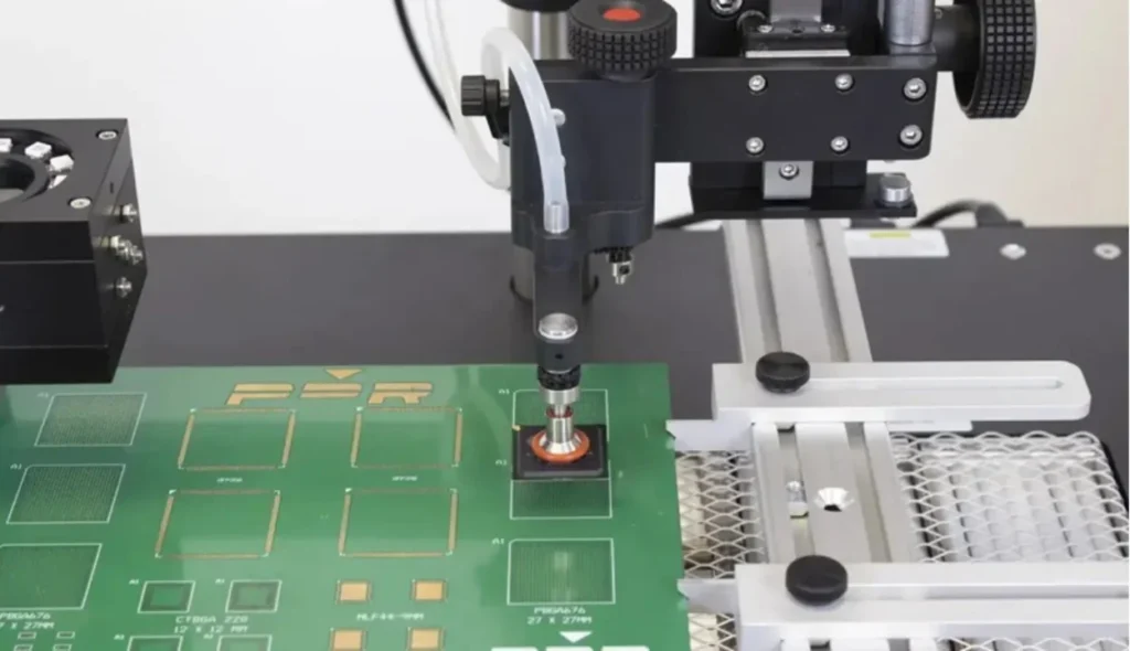
- Reballing or replacing the BGA component
- Reflowing the component with a controlled thermal profile
- X-ray inspection and electrical testing
The process is not simply “heat it and replace it.” A poorly controlled rework cycle can damage the laminate, lift pads, create voids, warp the board, or weaken nearby components.
Why BGA Rework Is More Difficult Than Standard SMD Repair
The biggest challenge is thermal control.
A BGA package needs enough heat to fully reflow all solder balls underneath the component. But the surrounding PCB, nearby components, internal copper planes, and package body all absorb heat differently. If the temperature is too low, some joints may not reflow completely. If it is too high, the board or package may be damaged.
This is especially difficult on boards with:
- Large ground or power planes
- Thick copper layers
- High layer count stackups
- Uneven copper distribution
- Large BGA packages
- Fine-pitch solder balls
- Heat-sensitive nearby components
Another issue is that the solder joints are hidden. A BGA can look perfectly aligned from the outside while having voids, bridges, head-in-pillow defects, or incomplete wetting underneath. This is why serious BGA rework should include X-ray inspection rather than relying only on external appearance.
Common Reasons BGA Rework Is Needed
BGA rework is usually required for one of four reasons.
The first is solder joint failure. This may include open joints, solder bridging, insufficient wetting, or head-in-pillow defects. These problems often come from poor paste printing, incorrect reflow profile, oxidation, board warpage, or component moisture issues.
The second is component replacement. During prototype development, engineers may need to replace a processor, FPGA, memory device, RF IC, or power management chip after a design change or component failure.
The third is assembly process debugging. If several boards show the same BGA issue, rework may help confirm whether the failure is caused by the component, PCB footprint, stencil aperture, reflow profile, or handling process.
The fourth is shortage-driven substitution. When a direct replacement is unavailable, a team may test an alternate part with the same footprint. In this case, rework becomes part of engineering validation, not just repair.
The Role of BGA Type in Rework Difficulty
Not every BGA behaves the same during rework. The BGA type matters because package construction affects heat absorption, warpage behavior, solder ball geometry, and inspection difficulty.
For example, a small memory BGA may be relatively manageable if the board is thin and the surrounding layout is simple. A large FPGA, high-pin-count processor, or package-on-package structure is much more demanding. Larger packages are more sensitive to temperature gradients across the component body. If one side reaches reflow before the other, package warpage may increase and create open joints.
Fine-pitch BGAs also leave less process margin. Small variations in solder volume, pad finish, component coplanarity, or placement accuracy can become real defects after reflow. This is why rework should not be evaluated only by whether the technician can remove and replace the chip. The more important question is whether the process can repeatedly produce reliable joints.
When BGA Rework Makes Sense
BGA rework makes sense when the board value is high, the failure is isolated, and the root cause is understood.
For example, rework is often reasonable when:
- A prototype board contains expensive components
- Only one BGA component is defective
- The PCB pads are intact
- The board has not gone through too many thermal cycles
- X-ray inspection is available after rework
- The reworked board will be used for engineering validation, not final shipment
In early-stage development, BGA rework can be extremely valuable. It allows engineers to test a revised component, recover a failed prototype, or continue firmware and system testing without waiting for a full rebuild.
It can also make sense for low-volume industrial or medical electronics if the rework process is controlled, documented, inspected, and approved according to the product’s quality requirements.
When Rework Is the Wrong Choice
Rework is not always the right answer.
If the PCB pads are damaged, the laminate is discolored, the board has visible warpage, or the same BGA location has already been reworked multiple times, the risk increases quickly. Even if the board passes a basic electrical test, long-term reliability may be compromised.
Rework is also a poor solution when the real problem is systemic. If multiple boards show the same BGA defect, the issue is probably not a one-off assembly mistake. It may be a stencil design problem, insufficient preheat, moisture-sensitive component handling failure, incorrect pad design, poor solder paste selection, or PCB fabrication issue.
In that situation, repairing individual boards may hide the real failure mode. The better approach is to stop and review the process data: paste inspection results, placement records, reflow profile, X-ray images, PCB flatness, component storage conditions, and pad finish quality.
Key Process Controls for Reliable BGA Rework
Reliable BGA rework depends on controlling the process, not just operator experience.
A proper rework process should include a defined thermal profile. The profile must account for preheat, soak, time above liquidus, peak temperature, and cooling rate. Too much thermal shock can damage the PCB or component. Too little heat can leave weak or partially reflowed joints.
Moisture control is also important. Many BGA packages are moisture-sensitive. If a component absorbs moisture and is heated too quickly, internal package damage or “popcorning” can occur. Components should be stored, baked, and handled according to their moisture sensitivity level.
Pad cleaning must be done carefully. Excessive mechanical force can lift pads or damage solder mask between pads. On fine-pitch BGAs, even small pad damage can make reliable replacement difficult.
Inspection should include X-ray whenever the assembly risk justifies it. X-ray can reveal bridging, voiding, missing balls, misalignment, and some head-in-pillow indicators. For critical products, electrical testing alone is not enough because a marginal joint may pass initially and fail later under thermal cycling or vibration.
Design Choices That Make BGA Rework Easier
Good BGA rework starts long before the board reaches the repair station. PCB design decisions can make rework easier or almost impossible.
Engineers should leave enough clearance around large BGA components for rework nozzles and localized heating. Placing tall connectors, shields, or heat-sensitive components too close to the BGA can create access problems.
Copper balance also matters. Heavy copper or large planes under one side of the package can cause uneven heating. That may create package tilt, incomplete reflow, or localized stress.
Clear fiducials, accurate solder mask registration, and well-designed pad geometry also help. For fine-pitch BGAs, small errors in footprint design can reduce assembly yield and make rework less reliable.
Thermal vias under or near BGA pads should be reviewed carefully. Via-in-pad designs need proper filling and plating. Open vias can wick solder away from the joint, causing insufficient solder volume.
What to Ask Before Approving BGA Rework
Before approving BGA rework, engineers should ask several practical questions.
Has the root cause been identified, or are we just replacing the part and hoping the issue disappears?
Are the PCB pads still in good condition?
How many thermal cycles has this board already experienced?
Will the board be used for lab validation, customer shipment, or regulatory testing?
Is X-ray inspection available after rework?
Can the supplier provide rework records, thermal profiles, and inspection results?
These questions are especially important when working with a BGA assembly manufacturer on production-intent hardware. A capable supplier should be able to explain not only how they rework the component, but how they prevent the same defect from appearing again in the next build.
Rework Should Feed Back Into the Assembly Process
The best rework programs do not treat repair as a separate activity. They use rework findings to improve the main assembly process.
If X-ray shows head-in-pillow defects, the team should review warpage, paste volume, component oxidation, and reflow soak conditions. If voiding is excessive, they should review stencil design, paste type, via placement, and reflow atmosphere. If bridges appear at one edge of the package, they should check placement accuracy, board flatness, and thermal uniformity.
Every rework event contains process information. When that information is documented and fed back into DFM, stencil design, and reflow profiling, future builds become more stable.
Final Thoughts
BGA rework is not just a repair skill. It is a controlled engineering process that sits between PCB design, assembly process control, inspection, and reliability management.
Used correctly, it can save expensive prototypes, support design iteration, and help teams understand hidden assembly problems. Used casually, it can create boards that pass today and fail later.
For high-value electronics, the real goal is not to become good at reworking BGAs. The goal is to understand why the BGA failed, confirm whether rework is technically justified, and use the findings to improve the next build.