
The conductivity of semiconductors mainly depends on the concentration of free electrons present in the material. Unlike conductors, where large numbers of electrons move freely, or insulators, where the count is small, semiconductors have a moderate level of free charge carriers. The key difference is that in materials like germanium and silicon, valence electrons are trapped within bonds between adjacent atoms, making them less mobile.
The crystal structures of these three-dimensional units allow for a repeating pattern that influences their conductance and resistance. Commonly used in electronic components, semiconductors exhibit a density of charge carriers that shifts based on external factors. Their electrical behavior is unique, with a balance between high conductivity, like metals, and low conductivity, like insulators, making them essential for modern technology.
How semiconductors allow electricity to flow
Every semiconductor has a specific electronic structure that determines how well it can conduct electricity. In materials like germanium and silicon, each atom has a nucleus surrounded by 32 electrons in a precise configuration. These electrons participate in covalent bonds, linking them to adjacent atoms, forming a stable crystal structure. The valence electrons are tightly bound, preventing them from moving freely, which limits conductivity under normal temperatures.
At absolute zero, a semiconductor behaves like an insulator since no free charge carriers are available to move. However, at room temperature (300oK), thermal energy causes some covalent bonds to break, releasing electrons and creating vacant spots known as holes. Each broken bond means one electron leaves, allowing a chain reaction that helps the material conduct to some extent. The energy needed for this process is 0.72 eV in germanium and 1.1 eV in silicon.
This process is influenced by the ionic and inert nature of the core structure, where the positive charge of the +4 charges plays a role. Since the crystal lattice remains intact, only a small number of carriers are generated, allowing the material to function as a controlled conductor. The ability of semiconductors to switch between insulating and conducting states makes them essential in electronics, as they serve key roles in modern devices. You can also read difference between semiconductors and superconductors
How holes and electrons move in a semiconductor
In a semiconductor, both electrons and holes act as carriers of electricity. When an incomplete bond exists in the crystal, a hole is created, allowing nearby electrons to move and fill it. As an electron leaves its previous position, it creates another hole, making the movement continuous. This process plays a key role in how a semiconductor conducts electricity.

As this mechanism continues, each time a hole is filled, a new one is created in a different spot. This gives the impression that holes are moving in the opposite direction of the electrons’ movement. In reality, it is the electrons that shift from one position to another, but the visualized effect makes it seem like the holes themselves are moving. This movement of charge is what enables semiconductors to work efficiently.
The significance of this process is that it allows semiconductors to rely on both types of charge carriers. The movement of electrons and holes within the neighborhood of atoms ensures continuous conductivity. Since the second hole is always occupied, the system remains active in conducting electricity. This dynamic nature of charge movement is what makes semiconductors highly valuable in modern electronics.
Charge Movement in Semiconductors
In a crystal, both electron-hole pairs and charge carriers play a major role in conductivity. The number of free electrons and holes determines the magnitude of the current flowing through the material. The mobility of electrons (μh) and holes influences how charge moves under an applied field. As a result, the direction of hole movement is opposite to that of electron movement.
The temperature directly impacts the rate of charge carrier creation and recombination. As temperature increases, the concentration of electron-hole pairs also increases, improving current flow. However, when temperature decreases, recombination reduces the free charge carriers, leading to lower conductivity. In an ideal semiconductor, this balance determines the overall charge density.
When an electric field is applied, electrons drift in the opposite direction, while holes move forward. The drifting of these carriers contributes to a sum of two currents, forming the total resultant current density.
The equation J = Jh + Je explains how the arithmetic combination of hole and electron drift leads to the overall charge-carrying capability.
The equation also shows how σ (conductivity) is linked to the sum of individual electron and hole contributions. In a unit volume, the concentration of carriers influences the magnitude of charge flow.
The total σ is calculated as σ = (σp + σn), where σp and σn represent hole and electron contributions. This confirms that both charge carriers are essential for conduction.
By using visualization, it becomes clear that semiconductors provide a unique way to control current. The backward movement of electrons and the forward motion of holes ensure a steady flow of charge. This controlled drifting makes semiconductors the foundation of modern electronic devices, as they regulate charge movement efficiently.
Impact of Temperature on Conductivity of Semiconductor
In a pure semiconductor, the number of free electrons and holes is equal, represented as n = p = ni. When the temperature increases, the concentration of charge carriers also increases, improving the conductivity. This relationship is characterized by a particular equation.
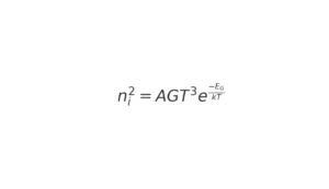
where T represents temperature on the Kelvin scale. The relation shows that charge carriers increase exponentially with rising temperatures.
The effect is noticeable in germanium, where conductivity rises by 6% for every degree centigrade increase. In silicon, this increase is about 8%, making these materials highly sensitive to heat changes. This phenomenon impacts the performance of semiconductor devices, requiring special care in operation. If the temperature goes beyond a certain limit, the effects can cause device failure.
This thermal variation is both a challenge and an advantage in electronic applications. Some specially designed transducers use this characteristic for measuring temperature changes. These devices are called thermistors, and they help regulate circuits based on heat levels. The given thermal behavior of semiconductors plays a crucial role in designing high-performance electronics.
By understanding these thermal properties, engineers can develop intrinsic systems that adapt to rapidly changing conditions. Proper care in semiconductor design ensures optimal operation without compromising reliability. Managing charge concentration and balancing n and p-levels remain critical factors in developing efficient semiconductor-based solutions.