
Introduction
The avalanche photodiode (APD) is a highly responsive semiconductor device that converts light into electric signals using the photoelectric effect. First designed in 1952 by the Japanese engineer Jun-ichi Nishizawa, the APD has become a key component in various applications, especially in fiber-optic communication systems. In recent years, graphene layers have been added to these diodes to help maintain their efficiency and avoid degradation, ensuring they continue to perform well over time.
The APD operates through the avalanche process, where photons collide with the diode, generating electrons and producing an electric current. This makes it an ideal choice for systems that require electrical signals from light particles. By improving the charge carrier generation, the APD is able to efficiently handle high-speed communication, making it crucial for modern systems and producers of electrical signals in various industries.
What is an Avalanche Photodiode?
An avalanche photodiode (APD) is a sensitive type of semiconductor that uses the photovoltaic effect to convert light into electricity. It operates under high reverse bias voltage, near the breakdown voltage, which allows charge carriers to multiply through avalanche breakdown. This process makes it ideal for the detection of small amounts of light, unlike solar cells that focus on generating power from light.
The APD is often used in applications like fiber-optic telecommunication, laser rangefinders, and positron emission tomography. It functions similarly to photomultiplier tubes, but instead of amplifying light to generate power, it is designed to detect incoming photons. These features make it crucial in fields such as particle physics and other applications where precise detection of light signals is needed. You can also read about step recovery diode.
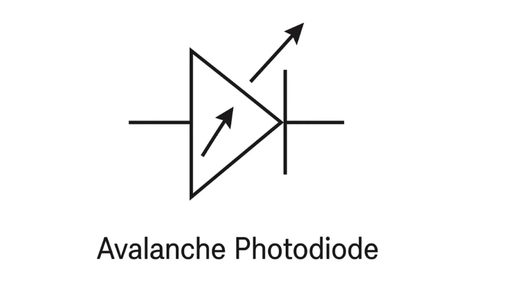
Avalanche Photodiode symbol
Avalanche Photodiode Construction
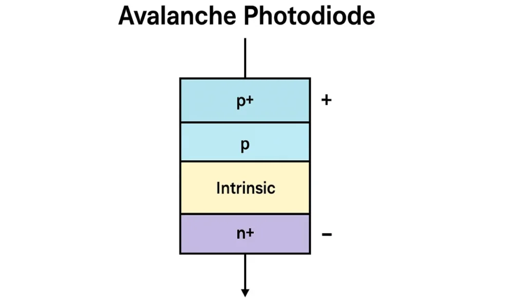
The construction of an avalanche photodiode is similar to a PIN photodiode, but it has a unique setup that allows it to work in a high range under reverse bias conditions. It consists of two heavily doped regions, P+ and N+, and two lightly doped regions, I and P, which form the intrinsic region. In this region, the depletion layer is thinner compared to a typical PIN photodiode, which helps in the efficient avalanche multiplication of the charge carriers created by the light impact or photon. The P+ region acts as the anode, while the N+ region serves as the cathode, and this action enhances the sensitivity of the photodiode, allowing the gain to be increased several times over other types of photodiodes. You can also read about varactor diode.
Working Principle
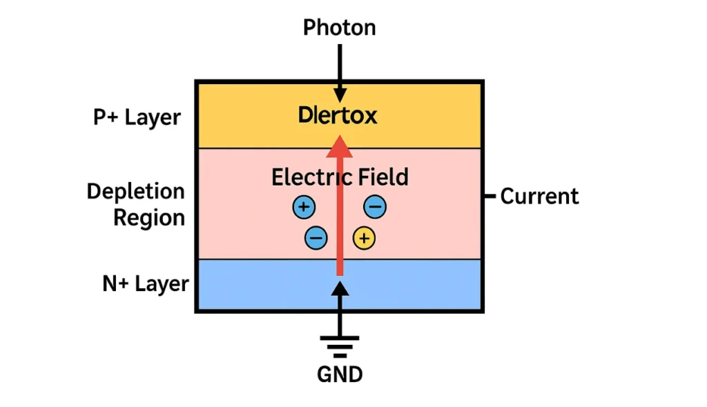
The working principle of an avalanche photodiode involves the generation of charge carriers when incident light hits the p+ region. This light gets absorbed by the resistive p region, creating electron-hole pairs. When a reverse voltage is applied, it creates a strong electric field across the depletion layer, which accelerates the charge carriers. These charge carriers move towards the pn+ region, where they gain enough velocity to collide with other atoms, causing more electron-hole pairs to form, a process known as avalanche breakdown. This leads to a high photocurrent, making the photodiode highly sensitive.
Principle of Operation
The principle of operation of an avalanche photodiode (APD) starts when photons hit the semiconductor material, providing energy to separate charge carriers into positive and negative pairs. These charge carriers are then accelerated by the applied electric field created by a reverse bias voltage, which causes them to move toward the space-charge boundary. As the charge carriers travel, they gain velocity and collide with other atoms, resulting in impact ionization and the creation of more electron-hole pairs. This process leads to avalanche breakdown, which greatly increases the charge flow and photocurrent in the diode.
The gain factor of the APD is affected by factors like doping, temperature, and the multiplication coefficient (α), which influence the number of electron-hole pairs generated. The reverse voltage applied controls the gain, with typical silicon APDs operating in the range of 100–200 V, achieving a gain of around 100. By employing structural techniques like doping profile adjustments, it is possible to increase the reverse voltage to 1500 V and achieve much higher gains and multiplication factors (M), making the APD highly sensitive and stable even under varying conditions.
Avalanche Photodiode in Optical Fiber Communication
In optical fiber communication (OFC), avalanche photodiodes are used to detect weak signals effectively. These diodes help improve the signal-to-noise ratio (S/N), ensuring that the signal is clear and distinguishable from noise. To achieve the best performance, the quantum efficiency should be high, as this ensures the photocurrent is maximized and most of the signals are noticed. By optimizing circuits and minimizing amplifier noise power, the photodetector’s power can be efficiently managed for a better signal-to-noise ratio.
Avalanche Photodiode Characteristics
Avalanche photodiodes are high-speed and sensitive devices that work by applying a reverse voltage to enhance their internal gain. They are designed for high sensitivity, making them ideal for applications like optical communication and optical distance measurement. Compared to a PIN-type photodiode, they excel at detecting low-range light and are especially effective in the near-infrared and short wavelengths. These diodes are crucial for long-distance communications and are available in different avalanche photodiode families to suit various needs.
What is the Difference Between PIN Photodiode and Avalanche Photodiode?
| Feature | PIN Photodiode | Avalanche Photodiode |
|---|---|---|
| Layers | P+, I, N+ | P+, I, P, N+ |
| Response Time | Low | High |
| Output Current | Multiplication of carrier current | Low |
| Internal Gain | Insignificant | 200 dB |
| Sensitivity | Low | High |
| Noise | Low | High |
| Reverse Bias Voltage | Low | High |
| Temperature Stability | Low-temperature stability | High-temperature stability |
| Amplifier Requirement | Mandatory | Not necessary due to available gain |
Advantages & Disadvantages of Avalanche photodiodes
Advantages:
High performance and quick response times make it ideal for precise applications.
Sensitivity range is high, allowing for the detection of weak signals.
Can detect low-intensity light, even at very low levels.
A single photon can generate many charge-carrier pairs, improving sensitivity.
High voltage can be applied, which allows for gain level control.
Disadvantages:
Operating voltage is high, requiring careful management.
Output is not linear, making it less suitable for certain applications.
Produces a high range of noise, which can affect signal clarity.
Lower reliability means it is less convenient for regular use.
It uses a reverse bias for proper operation, which may lead to stability issues.
Applications of Avalanche photodiodes
Avalanche photodiodes are used in optical fiber communications (OFC) to enhance receivers and improve signal detection.
They have a wide bandwidth, making them suitable for a variety of communication systems.
Laser rangefinders use these diodes to measure distances accurately.
Commonly found in PET scanners and barcode readers for precise imaging and scanning.
They are used in laser microscopy for detailed, high-resolution imaging.
Speed guns use these diodes to detect the speed of moving objects.
OTDR (Optical-Time Domain Reflectometers) utilizes avalanche photodiodes for testing the integrity of optical fibers.
Laser scanners rely on avalanche photodiodes for high-precision scanning of objects.
High sensitivity and charge carrier pairs formed in response to radiation make them crucial for optical communication.
Conclusion
Avalanche photodiodes (APDs) are highly sensitive and efficient devices, crucial for applications like optical fiber communication and laser rangefinders. Their ability to detect low-intensity light and operate under high reverse bias voltage makes them ideal for high-speed communication systems. With advancements in graphene layers and structural techniques, APDs continue to improve in performance, providing high sensitivity and stability even in challenging environments. Despite their high voltage requirements and some limitations, APDs remain a key component in modern detection systems.